
Serial Peripheral Interface or SPI is a synchronous serial communication protocol that provides full – duplex communication at very high speeds. Serial Peripheral Interface (SPI) is a master – slave type protocol that provides a simple and low cost interface between a microcontroller and its peripherals.
SPI Interface bus is commonly used for interfacing microprocessor or microcontroller with memory like EEPROM, RTC (Real Time Clock), ADC (Analog – to – Digital Converters), DAC (Digital – to – Analog Converters), displays like LCDs, Audio ICs, sensors like temperature and pressure, memory cards like MMC or SD Cards or even other microcontrollers.
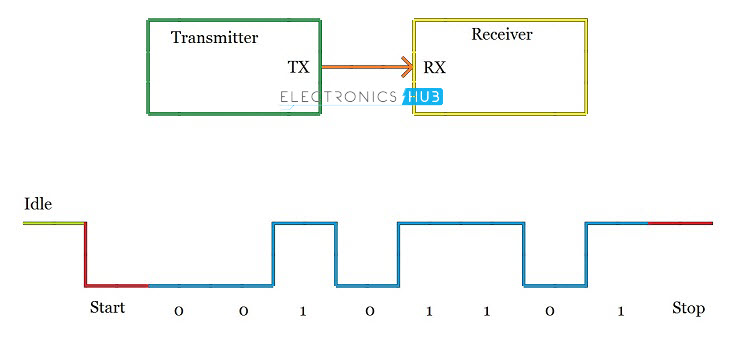
We have seen about UART in the previous article. In UART (or any common serial port), where the communication happens over RX and TX line, there is no clock signal i.e. it is an asynchronous communication. In this type of communication, there is no control over the data sent or whether the transmitter and receiver have same data rates.
In order to overcome this, UART uses synchronisation bits i.e. Start bit and Stop bits and also a pre agreed data transfer speeds (typically 9600 bps). If the baud rates of transmitter and receiver are not matched, the data sent from the transmitter will not reach the receiver properly and often garbage or junk values are received.

For short distance communication, Synchronous Serial Communication would be a better choice and in that Serial Peripheral Interface or SPI in particular is the best choice. When we say short distance communication, it often means communication with in a device or between the devices on the same board (PCB).
The other type of Synchronous Serial Communication Protocol is I2C (Inter – Integrated Communication, often called as I Squared C or I Two C). For this article, we will focus on SPI.
SPI is a Synchronous type serial communication i.e. it uses a dedicated clock signal to synchronise the transmitter and receiver or Master and Slave, speaking in SPI terms. The transmitter and receiver are connected with separate data and clock lines and the clock signal will help the receiver when to look for data on the bus.
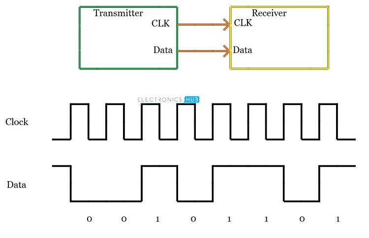
The clock signal must be supplied by the Master to the slave (or all the slaves in case of multiple slave setup). There are two types of triggering mechanisms on the clock signal that are used to intimate the receiver about the data: Edge Triggering and Level Triggering.
The most commonly used triggering is edge triggering and there are two types: rising edge (low to high transition on the clock) and falling edge (high to low transition). Depending on how the receiver is configured, up on detecting the edge, the receiver will look for data on the data bus from the next bit. S
Since both the clock and data are sent by the Master (or transmitter), we need not worry about the speed of data transfer.
What makes SPI so popular among other Synchronous Serial Communication protocols (or any serial communication for that matter) is that it provides a high speed secured data transfer with reasonably simple hardware like shift registers at relatively less cost.
SPI or Serial Peripheral Interface was developed by Motorola in the 1980’s as a standard, low – cost and reliable interface between the Microcontroller (microcontrollers by Motorola in the beginning) and its peripheral ICs.
Because of its simple interface, flexibility and ease of use, SPI has become a standard and soon other semiconductor manufacturers started implementing it in their chips.
In SPI protocol, the devices are connected in a Master – Slave relationship in a multi – point interface. In this type of interface, one device is considered the Master of the bus (usually a Microcontroller) and all the other devices (peripheral ICs or even other Microcontrollers) are considered as slaves.
In SPI protocol, there can be only one master but many slave devices.
The SPI bus consists of 4 signals or pins. They are
NOTE: Different manufacturers uses different nomenclature for the SPI bus. Refer the data sheet for exact information.
Since, the SPI bus is implemented using 4 signals or wires, it is sometimes called as Four Wire Interface. Let us first see a simple interface between a single master and single slave that are connected using SPI protocol and then we will explain about the 4 wires.
The following image depicts a Master (Processor) connected to a Slave (Peripheral) using SPI bus.
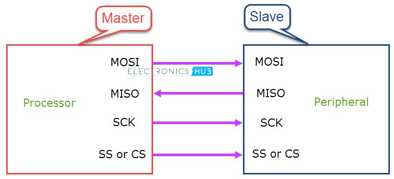
Master – Out / Slave – In or MOSI, as the name suggests, is the data generated by the Master and received by the Slave. Hence, MOSI pins on both the master and slave are connected together. Master – In / Slave – Out or MISO is the data generated by Slave and must be transmitted to Master.
MISO pins on both the master and slave are ties together. Even though the Signal in MISO is produced by the Slave, the line is controlled by the Master. The Master generates a clock signal at SCLK and is supplied to the clock input of the slave. Chip Select (CS) or Slave Select (SS) is used to select a particular slave by the master.
Since the clock is generated by the Master, the flow of data is controlled by the master. For every clock cycle, one bit of data is transmitted from master to slave and one bit of data is transmitted from slave to master.
This process happen simultaneously and after 8 clock cycles, a byte of data is transmitted in both directions and hence, SPI is a full – duplex communication.
If the data has to be transmitted by only one device, then the other device has to send something (even garbage or junk data) and it is up to the device whether the transmitted data is actual data or not.
This means that for every bit transmitted by one device, the other device has to send one bit data i.e. the Master simultaneously transmits data on MOSI line and receive data from slave on MISO line.
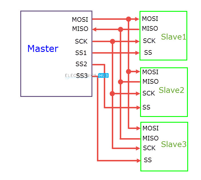
If the slave wants to transmit the data, the master has to generate the clock signal accordingly by knowing when the slave wants to send the data in advance. If more than one slave has to be connected to the master, then the setup will be something similar to the following image.
Even though multiple slaves are connected to the master in the SPI bus, only one slave will be active at any time. In order to select the slave, the master will pull down the SS (Slave Select) or CS (Chip Select) line of the corresponding slave.
Hence, there must by a separate CS pin on the Master corresponding to each of the slave device. We need to pull down the SS or CS line to select the slave because this line is active low.
The hardware requirement for implementing SPI is very simple when compared to UART and I2C. Consider a Master and a single Slave are connected using SPI bus. The following image shows the minimal system requirements for both the devices.
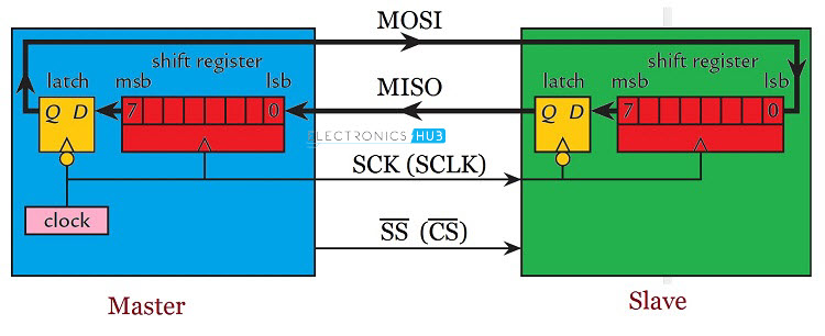
From the image, the Master device consists of a Shift Register, a data latch and a clock generator. The slave consists of similar hardware: a shift register and a data latch. Both the shift registers are connected to form a loop. Usually, the size of the register is 8 – bits but higher size registers of 16 – bits are also common.
During the positive edge of the clock signal, both the devices (master and slave) read input bit into LSB of the register. During the negative cycle of the clock signal, both the master and slave places a bit on its corresponding output from the MSB of the shift register.
Hence, for each clock cycle, a bit of data is transferred in each direction i.e. from master to slave and slave to master. So, for a byte of data to be transmitted from each device, it will take 8 clock cycles.
We have already seen that it is the job of the Master device to generate the clock signal and distribute it to the slave in order to synchronise the data between master and slave. The work of master doesn’t end at generating clock signal at a particular frequency.
In fact, the master and slave have to agree on certain synchronization protocols. For this, two features of the clock i.e. the Clock Polarity (CPOL or CKP) and Clock Phase (CPHA) come in to picture.
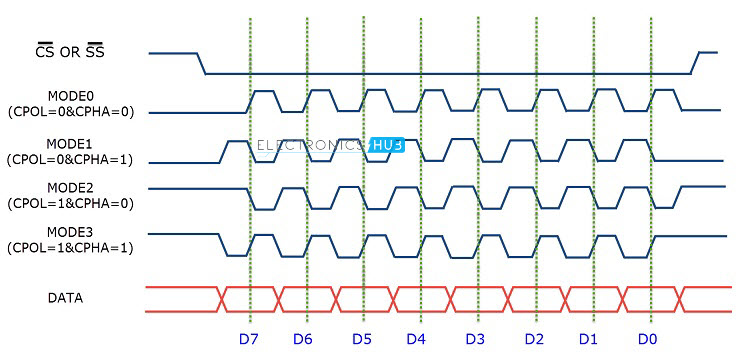
Clock Polarity determines the state of the clock. When CPOL is LOW, the clock generated by the Master i.e. SCK is LOW when idle and toggles to HIGH during active state (during a transfer). Similarly, when CPOL is HIGH, SCK is HIGH during idle and LOW during active state.
Clock Phase determines the clock transition i.e. rising (LOW to HIGH) or falling (HIGH to LOW), at which the data is transmitted. When CPHA is 0, the data is transmitted on the rising edge of the clock. Data is transmitted on the falling edge when CPHA is 1.
Depending on the values of Clock Polarity (CPOL) and Clock Phase (CPHA), there are 4 modes of operation of SPI: Modes 0 through 3.
Mode 0 occurs when Clock Polarity is LOW and Clock Phase is 0 (CPOL = 0 and CPHA = 0). During Mode 0, data transmission occurs during rising edge of the clock.
Mode 1 occurs when Clock Polarity is LOW and Clock Phase is 1 (CPOL = 0 and CPHA = 1). During Mode 1, data transmission occurs during falling edge of the clock.
Mode 2 occurs when Clock Polarity is HIGH and Clock Phase is 0 (CPOL = 1 and CPHA = 0). During Mode 2, data transmission occurs during rising edge of the clock.
Mode 3 occurs when Clock Polarity is HIGH and Clock Phase is 1 (CPOL = 1 and CPHA = 1). During Mode 3, data transmission occurs during rising edge of the clock.
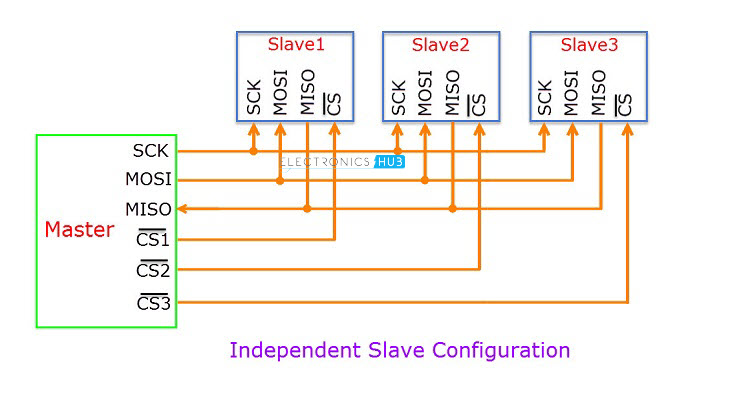
There are two types of configurations in which the SPI devices can be connected in an SPI bus. They are Independent Slave Configuration and Daisy Chain Configuration.
In Independent Slave Configuration, the master has dedicated Slave Select Lines for all the slaves and each slave can be selected individually. All the clock signals of the slaves are connected to the master SCK.
Similarly, all the MOSI pins of all the slaves are connected to the MOSI pin of the master and all the MISO pins of all the slaves are connected to the MISO pin of the master.
In Daisy Chain Configuration, only a single Slave Select line is connected to all the slaves. The MOSI of the master is connected to the MOSI of slave 1. MISO of slave 1 is connected to MOSI of slave 2 and so on. The MISO of the final slave is connected to the MISO of the master.
Consider the master transmits 3 bytes of data in to the SPI bus. First, the 1st byte of data is shifted to slave 1. When the 2nd byte of data reaches slave 1, the first byte is pushed in to slave 2.
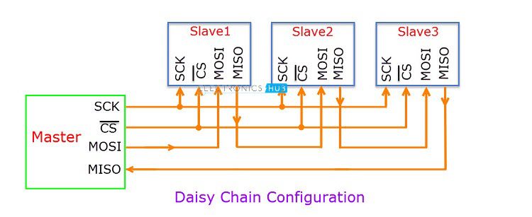
Finally, when the 3rd byte of data arrives in to the first slave, the 1st byte of data is shifted to slave 3 and the second byte of data is shifted in to second slave.If the master wants to retrieve information from the slaves, it has to send 3 bytes of junk data to the slaves so that the information in the slaves comes to the master.